
A few days ago I posted about one of my projects being a lithium polymer battery charger for a Raspberry Pi. I wanted to implement a feature to let me know what the battery charge level is to show the end user on an LCD (i.e. 100% charged, battery low etc.) My solution to this problem was very straight forward using a simple signal conditioning stage and an analog to digital converter with the successive approximation register architecture. This post will describe how these circuits work, and how I used them in my design.
The problem, simplified
All we need to do is detect the voltage on the battery and make some sense out of it. A typical way to do that is to use a voltage divider, a signal conditioning phase, feeding the result into an analog to digital converter, and then finally into your microcontroller.
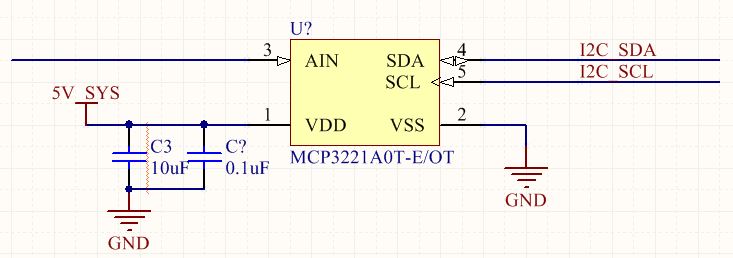
While typically selection an ADC will depend on a large amount of factors, this task doesn’t require a high sampling speed or very high resolution. Knowing this, I chose to use Microchip’s MCP3221. This ADC has:
- 12-bit resolution
- I2C (100kHz standard mode and 400kHz fast mode)
- SOT-23-5 package
- 2.7-5VDC input range
- single ended input channel
- Extremely cheap
All of these above characteristics made this the perfect fit for my application.
Now that we have the analog to digital converter picked out, all we really need to do is feed the sampled voltage to the chip. The data sheet states that the maximum input voltage for this chip is VDD+0.3, while VDD<5.5V. The battery voltage will never go over 4.2V due to the control scheme of the PMIC on board (and if it does we have bigger problems than worrying about displaying the battery percentage!). Don’t forget to add some decoupling capacitors near the VDD pins to ensure smooth power to the chip.
We can now just add a buffer op-amp with unity gain (gain equal to one which means Vout = Vin) and we’re finished!
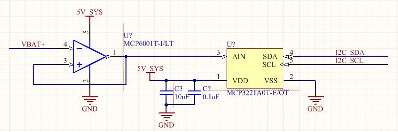
signal conditioning and ADC protection
I didn’t include any clamping diodes to protect the ADC as both the op-amp and ADC are both being powered with 5V. The op-amp will never output any voltage over 5V, which is within my ADC input limits. It is important to always consider the worst case scenarios when designing your circuitry. If I were truly sampling larger voltages, I would add a resistor divider network before my signal conditioning circuitry as well as add the Zener clamping diode and RC anti-aliasing filter to protect my ADC’s input. These extra passive components will definitely be less expensive than replacing an entire ADC chip, and doing so is overall good design practice.
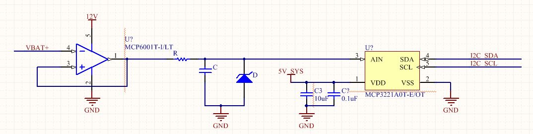
We use a buffer due to its near infinite input impedance, and extremely low output impedance. This helps us accurately measure the voltage on the line without distorting any of the input to the ADC. The anti-aliasing filter only helps to smooth the output of our op-amp before having it sampled at the input pin.
In my next post, I’ll go into detail over how this ADC works using an architecture called successive approximation to turn an analog waveform into a discrete digital signal.