One thing I’ve noticed as I gain experience in my professional career is the great lengths some companies go to hide technology from the user. This may seem to not make much sense, as you could easily say ‘but Adam, people see technology advance before them all the time. The jump from standard definition to HD, from HDDs to SSDs, the ever improving quality of my Snapchat selfies due to better cameras’. Well, yes…and no.
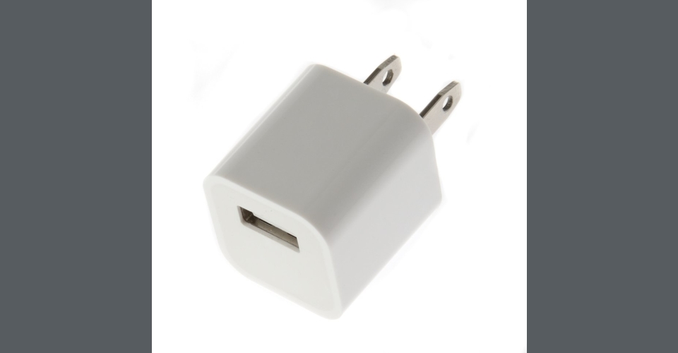
I’m going to talk about a piece of hardware that I have an appreciation as a design engineer for: the iPhone charger.
Yes, that’s right, the tiny little brick that everyone has plugged into their wall socket next to their night stand or at their desk at work. The amount of power electronics and safety design that went into your iPhone brick is truly astounding. The remainder of this article is going to explain the electrical portions of the charger.
Time to talk circuits
In short, your iPhone charger takes between 100 to 240VAC in, and provides a 5VDC output at 1A (5W) via a flyback switch mode power supply. Sounds simple enough, but the actual circuitry Apple has implemented into the charger shows that they engineered this thing to be as safe and efficient as possible. The breakdown of the power flow in the charger is as follows:
- The AC voltage enters into the charger and is rectified into HV DC by the use of a diode bridge rectifier.
- This newly rectified DC voltage is then fed into the flyback converter’s transformer (which is really an inductor but more on that in a later post), and converted to low voltage AC.
- The low voltage AC is the rectified back to DC using a high-speed Schottky diode.
- This low voltage is then passed through a pi filter to remove the ripple and switching transients from the converter and becomes the system output
- Like all modern SWPSs, the flyback converter is governed by an IC and a feedback loop monitoring the output voltage.
- Based on the target output voltage, the duty cycle is adjusted on the low side switching MOSFET to regulate the converter and achieve the desired voltage.
The schematic for the flyback stage is here:
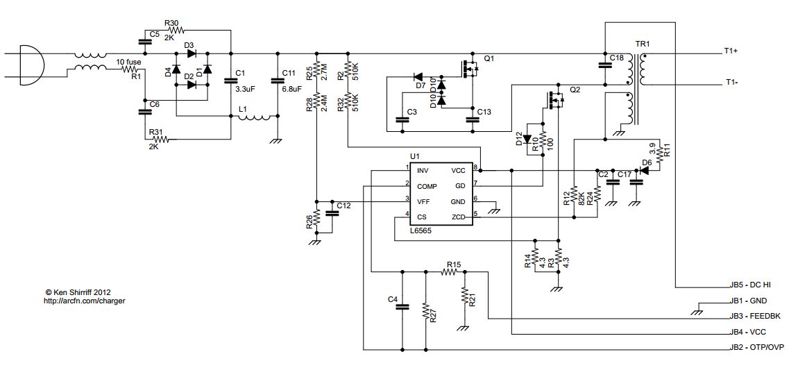
You can see the input choke, followed by the diode bridge rectifer, and two RC snubbers to reduce EMI from the DBR. The controller in this charger is the STMicroelectronics L6565.
The two small 4.3 Ohm current sense resistors measure the primary winding’s current, while the second winding on the primary side (aka auxiliary winding) measures the transformer demagnetization and provides the DC (with the help of a diode and capacitor) to power the controller IC.
You may be wondering how the controller IC first starts if the converter cannot begin to work until the switching FET is toggled! This is where resistors R2 and R32 come into play. These are start-up resistors, and provide the VCC needed to start the IC before the auxiliary winding can begin to provide power to the pin.
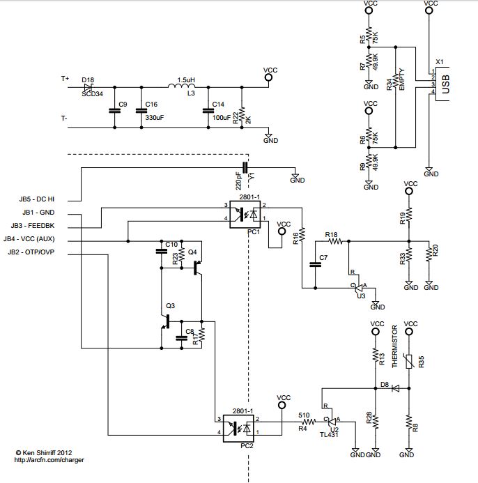
Apple has separated the high voltage and low voltage of the power stage onto two boards within the iPhone charger, and even added some opto-couplers to provide isolation of the feedback signals. These boards are interfaced together with a small ribbon cable carrying feedback signals such as primary current sense, output voltage, and DC input into the controller IC. That part of the circuit is shown here:
You know how when you plug in a non-Apple USB cable, you tend to get the message telling you that this device is not an authentic Apple device and may not work properly? Your phone can tell quite a bit of information based on the resistors placed on the USB D+/D- lines. This is based off of the USB Battery Charging standard, which I’ll get into later. Essentially, the voltage on these pins can tell a device what current to expect (i.e. 5A fast charge, standard USB 1A), whether the device plugged in is a standard or non-standard charging device, and more. Several manufacturers have taken to providing their own resistor values to their chargers to optimize their performance.
I’ll get into the USB BC1.2 standard in a separate post of its own.
Cheap knock off chargers that you can buy from gas stations, BestBuy, Amazon etc. do not follow the same design guidelines and practices as Apple does. I’m actually very interested in running an experiment where I fully charge my phone from 0% to 100% using an authorized Apple charger and a knock off and comparing the time it takes to charge and the temperature of the charger housing itself to see the difference the extra care in electronics design makes.
I hope you can come away from this post knowing at least a little bit more about that magical little 1”cubed brick we all use, and have a little bit more appreciation of it like I did when I first learned what all is inside.
The guys over at righto.com have done a really great in depth break-down of the charger, which I definitely recommend checking out if you’re super curious about the electrical details of the charger.