Successive Approximation Register Analog to Digital Converters

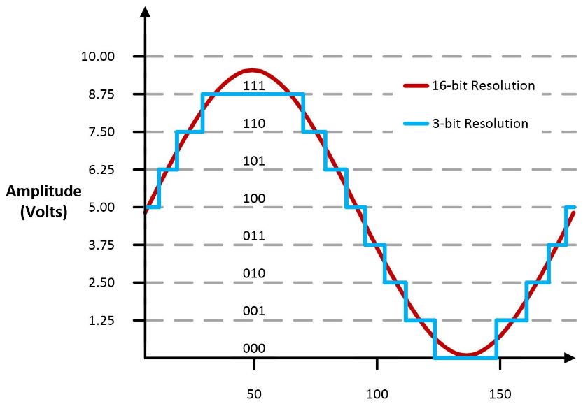
Converting the Physical into Digital

Analog to digital conversion is a critical part of electronics today. Everything from a digital scale at home to the most complex medical devices and satellites convert analog signals into digital representations. Today, I’m going to explain how one of the most popular ways to do this works, and how to take the digital output from an MCP3221 and convert it back into its analog, decimal representation.

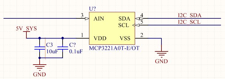
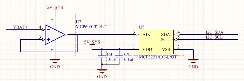
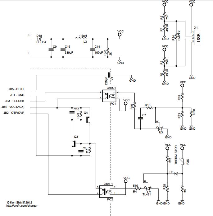
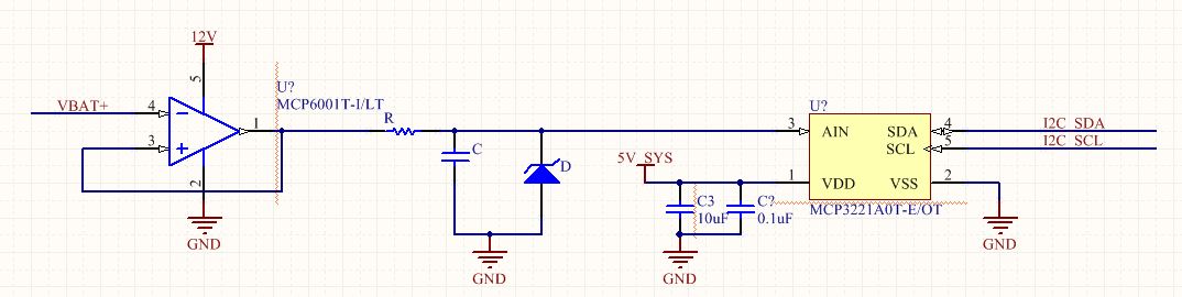
My previous post discussed a simple circuit to detect the battery voltage and feed it into an analog to digital converter. For reference, here is what a simple battery voltage detection circuit could look like:

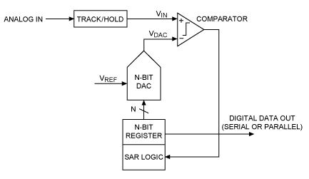
The MCP3221 ADC employs an extremely common architecture called a successive approximation register (SAR). An SAR ADC does exactly what its name states; it approximates the input voltage by successively comparing it to a known reference voltage, and determining if the measured voltage is higher or lower than this known reference voltage. The output is either a logic high or low based on the result of this comparison. This output is stored in a register that can then be read by your microcontroller/processor. This conversion is repeated as many times as there are bits of resolution; that is, for a 12-bit ADC like the MCP3221, this conversion takes place 12 times per input sampling before placing the result into the register to be read. Because of this, the internal circuitry could be operating at much higher frequencies than the ADC sampling rate.

Here is the block diagram of how the SAR algorithm works:

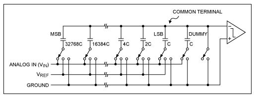
And here is the simplified internal circuitry for a 12-bit SAR ADC Notice the binary weighing of the capacitors; ideally each capacitor is exactly twice the value of the next smaller capacitor to give the highest accuracy possible:

Analog Successive Approximation

To begin, the analog input is sampled by switching the bottom plate of the capacitor network to ANALOG IN, while connecting the top plate to ground. This charges the capacitors and stores a binary scaled amount of energy on each capacitor. This can be seen by the binary weight of each successive capacitor in the example photo; from the MSB of 2^15(32,768) down to LSB of 2^0 (1). After sampling the input voltage, the common terminal is disconnected from ground, while the bottom plate is the switched to ground. This forces the common terminal to a voltage equal to -Vin.

The system then begins the binary searching, as the free terminal of the MSB is set to Vref while the remaining capacitors are still connected to ground. Using a simple binary summation and our knowledge of electronics, we see that this creates the capacitor equivalent of a resistor divider network, with Vcommon = -Vin + 0.5(Vref). We can see this is true by performing a simple nodal analysis on the top plate, and realizing that 2^11 == (2^10 + 2^9 + 2^8….+ 2^1 + 2^0) and therefore is 1/2 of the total capacitance.

This voltage is fed into the comparator, and will produce a logic high if Vin > 0.5(Vref), and a logic low if Vin < 0.5(Vin). If the result of the comparison is a logic high, the bottom plate of the MSB stays connected to Vref, otherwise it is connected back to ground. This result is stored in a register until the entire capacitor network has been checked, and the result can then be read by the microcontroller. The exact value of the voltage can then produce by using the successive approximation register and placing the logic highs and lows with their binary weight.

Making Sense of the Data

Now that we know how the device performs its analog successive approximation and stores the result, what happens when we want to make sense of this data? Lets say we have a 4-bit ADC and after sampling, the register has ‘1011’ as the stored result of our most recent conversion. This represents a decimal value of 1(2^3) + 0(2^2) + 1(2^1) + 1(2^0) = 8+0+2+1 = 9, but this is not our measured voltage!! The digital output produced by our MCP3221 is a function of the input signal and our supply voltage, VDD.

The least significant bit value is adjusted based on our supply voltage following the equation LSB SIZE = (VDD / 2^n) where ‘n’ is the number of bits on our ADC. Since I am supplying the 12-bit ADC with 5V, my LSB SIZE for the MCP3221 is 5V/(4096) = 0.001220703125. We can then perform some simple mathematics and get our true value for the measured voltage. Let’s see this in action…

Say our 12-bit ADC stored a value of all logic high (i.e. ‘1111 1111 1111 1111’). We expect this value to be equal to VDD, which in my case is 5V. We measured our LSB value above to be 0.001220703125. For brevity sake, I will call this value ‘Z’. To convert this digital value into its analog representation, we just plug in our values like so:

Z(2^15) + Z(2^14) + … + Z(2^1) + Z(2^0) = 2.5 + 1.25 + ….0.002441406 + 0.001220703125 = 4.998779V. Wait a second, why isn’t this exactly 5V as we predicted? In fact, this value is exactly ONE LSB Value away from being exactly 5V. This is where our DUMMY capacitor comes into play! Refer to the circuitry above, and you’ll see that next to our LSB capacitor of value ‘C’, we have another capacitor of the same value ‘C’ next to it. This capacitor is needed for our binary summation to work!

4.998779 + 0.001220703125 = 5.

We’ve done it! We can now convert an analog voltage into a digital representation using an analog successive approximation, and we now know how to convert THAT digital representation BACK into its analog value! How cool is that?? I hope this helped you understand how we can convert analog samples to and from the digital domain using this surprisingly simple, but very powerful, type of analog to digital converter.

How to Detect Battery Voltage

A few days ago I posted about one of my projects being a lithium polymer battery charger for a Raspberry Pi. I wanted to implement a feature to let me know what the battery charge level is to show the end user on an LCD (i.e. 100% charged, battery low etc.) My solution to this problem was very straight forward using a simple signal conditioning stage and an analog to digital converter with the successive approximation register architecture. This post will describe how these circuits work, and how I used them in my design.

The problem, simplified

All we need to do is detect the voltage on the battery and make some sense out of it. A typical way to do that is to use a voltage divider, a signal conditioning phase, feeding the result into an analog to digital converter, and then finally into your microcontroller.

While typically selection an ADC will depend on a large amount of factors, this task doesn’t require a high sampling speed or very high resolution. Knowing this, I chose to use Microchip’s MCP3221. This ADC has:

  • 12-bit resolution
  • I2C (100kHz standard mode and 400kHz fast mode)
  • SOT-23-5 package
  • 2.7-5VDC input range
  • single ended input channel
  • Extremely cheap

All of these above characteristics made this the perfect fit for my application.

Now that we have the analog to digital converter picked out, all we really need to do is feed the sampled voltage to the chip. The data sheet states that the maximum input voltage for this chip is VDD+0.3, while VDD<5.5V. The battery voltage will never go over 4.2V due to the control scheme of the PMIC on board (and if it does we have bigger problems than worrying about displaying the battery percentage!). Don’t forget to add some decoupling capacitors near the VDD pins to ensure smooth power to the chip.

We can now just add a buffer op-amp with unity gain (gain equal to one which means Vout = Vin) and we’re finished!

signal conditioning and ADC protection

I didn’t include any clamping diodes to protect the ADC as both the op-amp and ADC are both being powered with 5V. The op-amp will never output any voltage over 5V, which is within my ADC input limits. It is important to always consider the worst case scenarios when designing your circuitry. If I were truly sampling larger voltages, I would add a resistor divider network before my signal conditioning circuitry as well as add the Zener clamping diode and RC anti-aliasing filter to protect my ADC’s input. These extra passive components will definitely be less expensive than replacing an entire ADC chip, and doing so is overall good design practice.

We use a buffer due to its near infinite input impedance, and extremely low output impedance. This helps us accurately measure the voltage on the line without distorting any of the input to the ADC. The anti-aliasing filter only helps to smooth the output of our op-amp before having it sampled at the input pin.

In my next post, I’ll go into detail over how this ADC works using an architecture called successive approximation to turn an analog waveform into a discrete digital signal.

iPhone Charger Demystified

One thing I’ve noticed as I gain experience in my professional career is the great lengths some companies go to hide technology from the user. This may seem to not make much sense, as you could easily say ‘but Adam, people see technology advance before them all the time. The jump from standard definition to HD, from HDDs to SSDs, the ever improving quality of my Snapchat selfies due to better cameras’. Well, yes…and no.

I’m going to talk about a piece of hardware that I have an appreciation as a design engineer for: the iPhone charger.

Yes, that’s right, the tiny little brick that everyone has plugged into their wall socket next to their night stand or at their desk at work. The amount of power electronics and safety design that went into your iPhone brick is truly astounding. The remainder of this article is going to explain the electrical portions of the charger.

Time to talk circuits

In short, your iPhone charger takes between 100 to 240VAC in, and provides a 5VDC output at 1A (5W) via a flyback switch mode power supply. Sounds simple enough, but the actual circuitry Apple has implemented into the charger shows that they engineered this thing to be as safe and efficient as possible. The breakdown of the power flow in the charger is as follows:

  • The AC voltage enters into the charger and is rectified into HV DC by the use of a diode bridge rectifier.
  • This newly rectified DC voltage is then fed into the flyback converter’s transformer (which is really an inductor but more on that in a later post), and converted to low voltage AC.
  • The low voltage AC is the rectified back to DC using a high-speed Schottky diode.
  • This low voltage is then passed through a pi filter to remove the ripple and switching transients from the converter and becomes the system output
  • Like all modern SWPSs, the flyback converter is governed by an IC and a feedback loop monitoring the output voltage.
  • Based on the target output voltage, the duty cycle is adjusted on the low side switching MOSFET to regulate the converter and achieve the desired voltage.

The schematic for the flyback stage is here:

You can see the input choke, followed by the diode bridge rectifer, and two RC snubbers to reduce EMI from the DBR. The controller in this charger is the STMicroelectronics L6565.

The two small 4.3 Ohm current sense resistors measure the primary winding’s current, while the second winding on the primary side (aka auxiliary winding) measures the transformer demagnetization and provides the DC (with the help of a diode and capacitor) to power the controller IC.

You may be wondering how the controller IC first starts if the converter cannot begin to work until the switching FET is toggled! This is where resistors R2 and R32 come into play. These are start-up resistors, and provide the VCC needed to start the IC before the auxiliary winding can begin to provide power to the pin.

Apple has separated the high voltage and low voltage of the power stage onto two boards within the iPhone charger, and even added some opto-couplers to provide isolation of the feedback signals. These boards are interfaced together with a small ribbon cable carrying feedback signals such as primary current sense, output voltage, and DC input into the controller IC. That part of the circuit is shown here:

You know how when you plug in a non-Apple USB cable, you tend to get the message telling you that this device is not an authentic Apple device and may not work properly? Your phone can tell quite a bit of information based on the resistors placed on the USB D+/D- lines. This is based off of the USB Battery Charging standard, which I’ll get into later. Essentially, the voltage on these pins can tell a device what current to expect (i.e. 5A fast charge, standard USB 1A), whether the device plugged in is a standard or non-standard charging device, and more. Several manufacturers have taken to providing their own resistor values to their chargers to optimize their performance.

I’ll get into the USB BC1.2 standard in a separate post of its own.

Cheap knock off chargers that you can buy from gas stations, BestBuy, Amazon etc. do not follow the same design guidelines and practices as Apple does. I’m actually very interested in running an experiment where I fully charge my phone from 0% to 100% using an authorized Apple charger and a knock off and comparing the time it takes to charge and the temperature of the charger housing itself to see the difference the extra care in electronics design makes.

I hope you can come away from this post knowing at least a little bit more about that magical little 1”cubed brick we all use, and have a little bit more appreciation of it like I did when I first learned what all is inside.

The guys over at righto.com have done a really great in depth break-down of the charger, which I definitely recommend checking out if you’re super curious about the electrical details of the charger.

LiPo Battery Charger/UPS for a RaspberryPi

I’ve been becoming more and more interested in battery technology and battery management systems. I’ve also recently started doing some freelance electronics design work to keep my creativity going, have some fun, and make a little extra cash (Note: my current employer allows me to do this as long as it doesn’t interfere with my day job). A customer reached out to me on UpWork and asked if I could design two PCBs for a project he’s working on. They wanted a battery management system, and a sensor board to interface to his RaspberryPi and peripherals. Seeing as battery systems are my new-found interest, I jumped at the opportunity to learn a little bit more about the technology.

The requirements for the battery management system (henceforth ‘BMS’) were:

  • ability to simultaneously charge a 8000mAh LiPo battery and supply system power
  • provide uninterrupted power in the case of DC input cut-off
  • output 2.5-3A and supply 5V/3V3 to the system load (sensors, 7” LCD touchscreen etc.)
  • fit on a 30mm X 80mm dual layer PCB
  • ability to terminate power to the Raspberry Pi if needed
  • ability to determine approximate charge level
  • determine if powered from battery or wall-wart
  • 12V, 3.5A DC input

I did a little research and found the perfect chip for this project; the Texas Instruments BQ25895. This is a great little PMIC (power management integrated circuit) that is jam packed full of features that solve nearly all of the power requirements in a single package solution. The main features that caught my attention were:

  • output up to 3.1A at 5V on the output via a boost converter @ 1.5MHz switching
  • an I2C interface to a host (the RPi)
  • ability to dynamically swap power-sources (battery or DC input)
  • battery temperature monitoring
  • auto-detect USB SDP, CDP, DCP etc. (USB BC1.2 standard)
  • +/- 0.5% charge voltage regulation
  • small footprint (4mm x 4mm)

The high switching speeds on the boost converter means I could use a smaller inductor (more on this later), which is handy on projects that have very limited real estate such as this. The I2C interface allows for changing the power systems characteristics, TI’s PowerPath is perfect for making small UPSs, and battery protection/monitoring is critical for safety (fire is a no-no).

The BQ25895 combined with a 5V -> 3V Buck converter is sufficient to meet all of our power requirements for this little project. For this conversion, I chose to use the TI LM2831 to provide the 3.3V output and supply up to 1.5A.

Achieving the 3.3V output from the LM2831 is as easy as following the datasheet Texas Instruments supplies. I have provided my equations used to calculate the values for the input/output capacitors, inductor, diode and feedback resistors onto the schematic below.

With these two small chips, I can fulfill all of the power requirements my customer asked for in a cost effective, low part count solution. In the next post, I’ll explain some of the features this PMIC has, and how they’re useful.

A Look at What's to Come

It’s been a while since I’ve last posted on my site, but I’m back now and have tons of ideas for new content. I’ll definitely be focusing more on hardware design, break downs, and talking about some of my own projects that I have going on.

Some of the topics I’ll be covering in the near future are: - Lithium ion/Lithium polymer batteries - Charging circuitry and battery monitoring systems - Breaking down the iPhone brick charger - Switch mode power supplies (AC/DC, DC/DC) - Designing my own uninterrupted power supply and battery charger for a RaspberryPi - Hack-a-thon ideas and feasibility studies - DC Motors and motor control

And lots more. Look forward to sharing all of this with everyone!

Hardware Engineering - adam wheeler